
PCB, otherwise known as printed circuit panel is used for connecting through electricity the electrical parts with the usage of conductive pathways and indicate traces. These will go through etching from copper blankets that have been laminated to become non-conductive substrate. A certain PCB filled with electric components is called a published world board assembly or in short, PCB assembly. Produced enterprise panels are generally within virtually all the easiest gadgets which are commercially produced.
The development of PCB assembly started during the twentieth century. In 1903, Albert Hanson who was a German inventor gave a description regarding smooth foil conductors being laminated to an insulating board in numerous layers. Also in 1904, Thomas Edison built a research with the compound processes of plating conductors on a linen paper.
Additionally, in 1913, Arthur Berry created a patent of a print-and-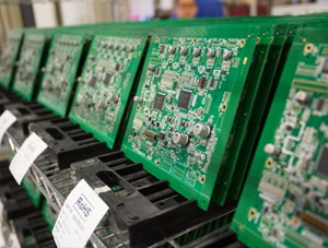 etch technique in Britain that Max Schoop obtained a patent in America. It absolutely was also in 1927 that Charles Durcase purchased a patent regarding the technique of electroplating signal patterns.
After the PCB assembly is finished, the electrical parts must certanly be linked therefore that a functional PCB assembly is formed. You can find two structure processes which may be used in order to form the PCB assembly. One may be the through-hole construction in that the aspect brings are put in the holes while another one could be the surface-mount construction where the parts are based on patches located on the external surfaces of the PCB. Equally kinds of construction have portion brings which are fixed mechanically along with electrically to the panel by way of a material solder which has melted.
PCB is needed for the physical help of any type of technology product. This really is in the form of a card or a table that will be comprised of thin metal or difficult plastic frequently referred to as the insulator. The chips of the digital tools are secured on this card or the board. The PCB is found in the smallest device just like the mobile to larger technology units such as the pc and the television. The PCB which has not been equipped with any element is called PCB as it’s raw but once the technology components are secured it is known as PCB assembly service.
In the modern world engineering is establishing at an easy rate so many improvements are taking place in the detailed operates of all of the technology devices therefore the majority of the technology devices which are of the old design is becoming obsolete and the components or the parts aren’t available easily. Only at that point it will become necessary to sometimes get a new product or update the present model of the electronics things whether at company or at home.
More over, there are numerous soldering solutions to be properly used to be able to join the PCB components to ensure that PCB assembly can be possible. Generation that’s of large size must certanly be done through device position and bulk wave type of soldering. However, expert experts have the capacity to solder really second pieces by the give below a microscope. That is often completed with the usage of tweezers and a soldering iron with an excellent hint which is made for small quantity prototypes. Yet, you can find parts which are difficult to solder with the fingers just as the ball grid array.
PCB’s which would constitute the PCB assembly have conformal covering that is applied through dipping or treating once the components are done soldering. This coat will generally prevent rust and the dripping of current or possible shorting due to condensation. PCB assembly is static painful and sensitive, thereby; it should be put inside antistatic bags whilst it will be transported. Incorrect techniques in handling could transmit fixed charge through the panel and consequently may injury the components.